It was the fall of 2021, and headlines were bristling with stories about the ongoing “chip choke.”
A group of Notre Dame engineering students taking a course called Integrated Circuit Fabrication, or IC Fab, followed the stories closely. Assembly lines were lurching back to life following the disruptions that came with the COVID-19 pandemic. However, many were stalled once again waiting for some of the tiniest components in the design of their products: semiconductor chips. Since the majority of the world’s most advanced semiconductors come from a single chip maker located on the island of Taiwan, there was no easy solution. Ford Motor Co. began filling acres of parking lots at Kentucky Speedway with new, nearly fully assembled Super Duty pickups, eventually amassing a stockpile so large it could be seen from space.
Stories of the chip choke left the public outraged and incredulous: How could a component as thin and narrow as a thumbnail stop multibillion-dollar industries in their tracks?
But for the Notre Dame students in IC Fab, the stories were something else: relatable. That is because they, too, were chip makers, and they were in the throes of a chip choke of their own.
Entering the Nanofabrication Lab
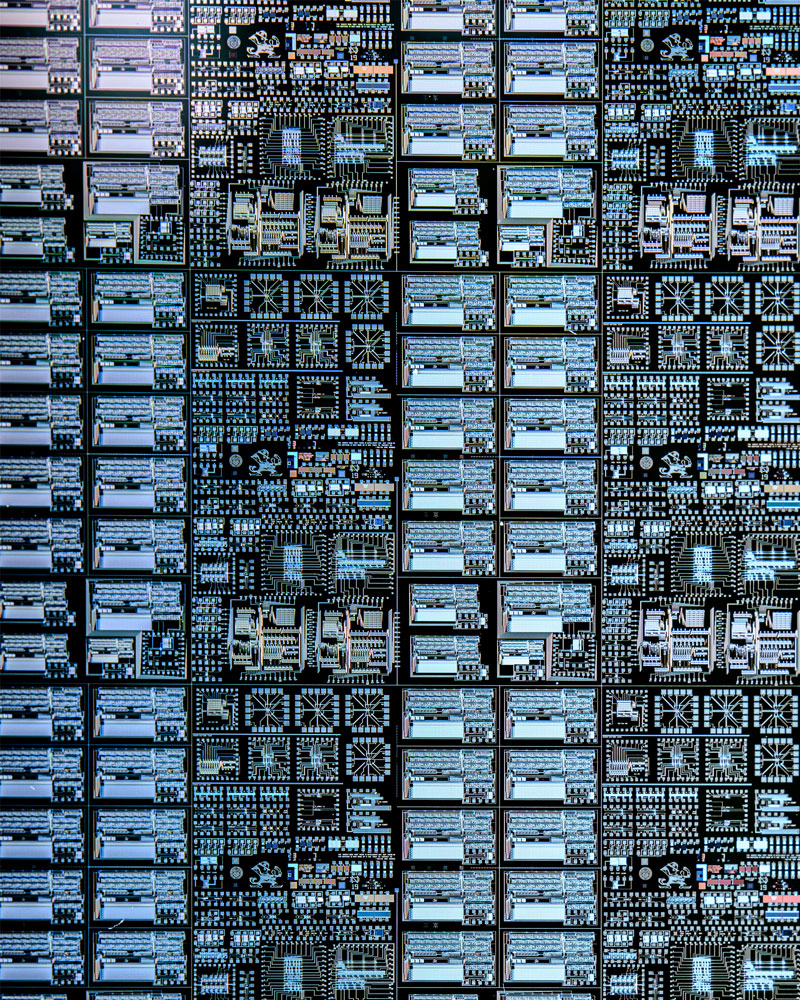
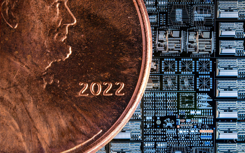
Behind IC Fab’s ordinary name lies a bold challenge. Each student begins the course with a pure crystalline slice of silicon, called a wafer. The students’ task is to learn and execute an intricate 35-step process over 11 weeks. If they are successful, then at the end of the course they will have transformed their wafers into 2-millimeter-by-3-millimeter 5,000-transistor chips capable of playing the well-known notes of Notre Dame’s fight song, the “Victory March.”
Few students are aware of the project that lies before them when they sign up for IC Fab—or that it will take them about 90 hours in the lab to complete it. Most are drawn to the lab itself.
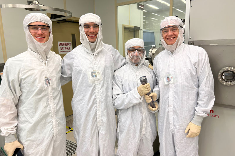
“I knew I wanted to work in the clean room at some point during my time at Notre Dame,” explains senior electrical engineering major Brennah Satterfield, who took IC Fab during fall 2021.
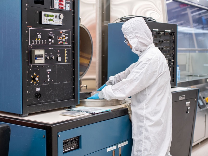
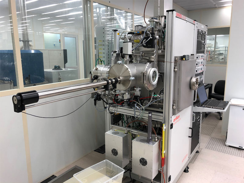
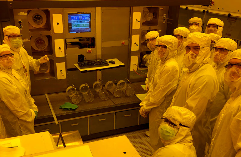
The facility known as the clean room has a more formal name: the Notre Dame Nanofabrication Facility. Part of the College of Engineering, it is one of Notre Dame’s core research facilities, but few undergraduates ever step inside it—though they often find themselves on the outside looking in. The 9,000-square-foot facility faces the large central atrium of Stinson-Remick Hall of Engineering, where many engineering majors take their first courses. They pass by often and wonder what the researchers inside are doing as they move under amber-colored lights, shrouded in what look like hazmat suits.
IC Fab is their main opportunity to find out. And before students have spent even their first hour inside the clean room, they discover some of the reasons it is so tightly controlled. “Clean” in the world of nanofabrication indicates a cleanliness far beyond that of a typical hospital’s surgical suite. Standards for the most sensitive areas of the clean room require there to be no more than 100 half-micron-sized particles in each cubic foot of air. Since the naked eye cannot see objects smaller than about 40 microns, this means a microscopic level of clean.
To maintain its standards for cleanliness, the clean room is carefully climate controlled and equipped with an elaborate air filtration system. But the key is not introducing contamination in the first place. Students learn to follow an intricate preparatory ritual before they enter. They vacuum and cover their shoes. They don hair nets, gloves, and goggles and top everything off with special static-free hooded coveralls.
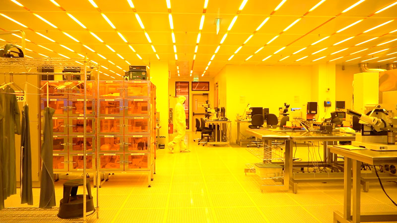
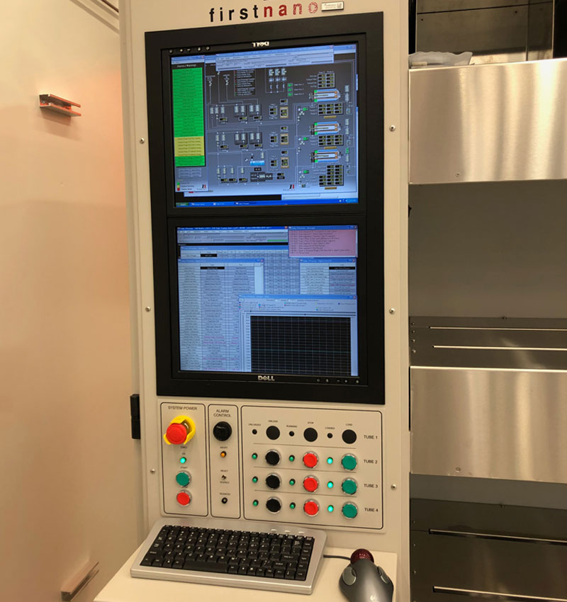
Inside the clean room, students also observe a rigorous set of safety measures for handling the acids they use to etch the chips and for operating furnaces hot enough to melt many metals.
Students maintain the safety and cleanliness standards not just out of concern for themselves and for their lab mates, but also for their wafers. After spending dozens of hours shepherding their wafer through delicate processes, handling them like fragile eggs, and etching intricate patterns onto them, students grow attached.
“By the end of the class, it’s like it’s your baby,” says senior electrical engineering major Sofia Main, who was also in the 2021 IC Fab cohort. “You find yourself saying things like, ‘Oh, wafer 4621, that’s my favorite.’”
Layer by layer
Of course, the inevitable does happen. Wafers crack in the furnace or students perform a process out of order. They get dropped—or simply are chipped as they are transferred from one machine to another. (Even a small nick on the perimeter of the wafer creates a stress point that weakens the wafer and makes it likely to cleave into pieces.) One student, at a critical point in the process, accidentally sneezed on his wafer.
Heartbreaking as mistakes can be, they are an important part of the process, says Alan Seabaugh, the Frank M. Freimann Professor of Electrical Engineering, who teaches IC Fab each fall.

“Students gain confidence from getting things right the first time,” he says, “but they also gain resilience by working through mistakes and by seeing that most of the time they can be remedied.”
Seabaugh, who also leads the center for Notre Dame Nanoscience and Technology at the University called NDnano, sets aside time in most class periods for troubleshooting. This allows students to work together to retrace their steps, discuss concerns they have about their wafers, and determine what steps to take as they move forward in the process.
“They learn that making a chip is, in a way, like oil painting: You work layer by layer, adding, patterning, and removing, and over time the picture emerges,” Seabaugh says. “Often it’s a matter of taking a step back and getting it right before you move to the next layer.”
To make sure all the equipment and materials are ready, Seabaugh and his graduate teaching assistants also work through the process with a few wafers of their own, staying a step ahead of the students. The clean room is available 24 hours a day to students taking the course, and Seabaugh is known to take FaceTime calls at home or make the trip to campus in the middle of the night to correct a particularly difficult problem. Teaching assistants and clean room staff also help the students at odd hours and on weekends to enable them to meet the tight deadlines imposed by the course.
“It’s a really tough challenge,” says electrical engineering major Collin Finnan, another member of the 2021 IC Fab cohort. “But you realize how much support you have, and that keeps you going even when you make mistakes and struggle to sort them out.”
For Finnan and the other students, another main source of support comes from the class’s team structure. Seabaugh assigns students to teams of three to ensure the students can help one another follow the cleanliness and safety protocols, remind each other how to follow the processes they learn in class, and—perhaps most importantly—support each other in making good decisions. The students in each group pool their wafers so if one or even two break, they can still see the process through to the last step.
“March on to victory”
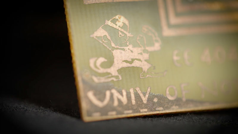
As students spend time in class gaining an understanding of the increasingly complex maze of layered materials, channels, and connections on their wafer, a few bits of Notre Dame insignia help them find their way. Students etch a tiny Notre Dame leprechaun, a silhouette of the Main Building’s Golden Dome, and an interlocked ND monogram onto the chip. By playing what sounds like a game of Battleship, students look at their wafers together, calling out things like, “Look at the ring oscillators two rows up from the Leprechaun.”
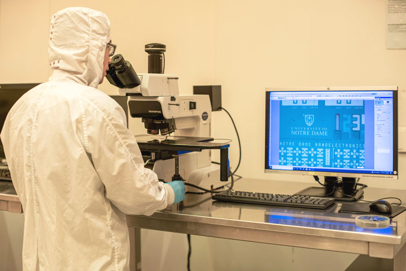
For many students, the most memorable moment of the class is when they not just see but also hear the effects of the circuitry carved into a working chip. They connect the chip to a power source and hear the familiar tune that goes with the lyrics:
Cheer, cheer for old Notre Dame,
Wake up the echoes cheering her name,
Send a volley cheer on high,
Shake down the thunder from the sky.
What though the odds be great or small
Old Notre Dame will win over all,
While her loyal sons and daughters
March on to victory.
The idea for the class’s musical conclusion emerged more than two decades ago and has undergone a gradual process of refinement. The initial concept came from a group of six senior undergraduate students who took a series of chip-based courses taught by Gary Bernstein, Gregory Snider, Jay Brockman, and Peter Kogge in the early 2000s. For their capstone project, the students figured out the frequencies and durations of all 65 notes that make up the main chorus of the fight song and designed several circuits to generate the sound. Snider, who was teaching IC Fab at the time, decided to integrate the idea into the course. With each iteration of the course, Snider refined the process and design, which, in turn, led to higher yields of sound chips.
Working with “original texts”
Students often find that taking IC Fab has an effect—sometimes a surprising one—on their plans for the future. As soon as he had completed IC Fab, Finnan dropped his second major so he could spend more time doing additional research in microelectronics and in the Nanofabrication Facility. Instead of looking for an industry job, as he had originally planned, he is bound for graduate school where he plans to continue his research.
Similarly, Satterfield shifted her focus to semiconductors after taking the course. She soon landed an important internship fabricating chips in a clean room and eventually a job offer to work in a lab testing chips.
For classmate Luis Hernandez, who is also a senior electrical engineering major, the course triggered a passion for semiconductor design.
“I had just transferred to Notre Dame when I took the class, and it was my first exposure to integrated circuits. But I was fascinated by all of it—the parts, the process, how everything comes together,” he says.
Hernandez now plans to get a job designing semiconductors. And although he will likely work with computer-aided design software rather than in the clean room with the chips themselves, he says he is grateful to have a deep understanding of how chips are made.
“Some designers have never actually made a chip,” he says, “but I think it is helpful to not just have a technical understanding but also to have firsthand experience and to have actually seen a chip come together layer by layer, to know how it is all intertwined and interconnected.”
Sofia Main plans to work in robotics rather than integrated circuits. Yet, she still credits the course with helping her find her path and forge her identity as an engineer.
“The class was the most hands-on work of any class I’ve taken, and it was daunting at first,” she says. “But it made me comfortable working in new situations and it made me confident that I can grow in a new area quickly.”
Seabaugh explains the confidence students gain in the course using an analogy with courses in the humanities. “In those courses, instructors have students work with original texts, so they know what it is like to handle primary material and not just read someone else’s interpretation. That’s similar to what we are doing here,” he says. “The students dig deep to learn these technologies for themselves, not by what others say. This broadens their understanding of what is possible.”
Integrated into the world of integrated circuits

There is nothing new about Notre Dame engineers being recruited into semiconductor jobs. As early as the 1950s, companies like Texas Instruments, where the integrated circuit was invented, were running ads in the Notre Dame Scholastic in hopes of luring Notre Dame graduates to join their ranks.
When the Semiconductor Research Corporation, a consortium made up of leading semiconductor companies, began funding research in the 1980s, one of its first funded projects was at Notre Dame. Since then it has funded three major research centers—the Midwest Institute for Nanoelectronics Discovery, the Center for Low Energy Systems Technology, and the Applications and Systems-Driven Center for Energy-Efficient Integrated NanoTechnologies—at the University over a 15-year span.
Interestingly, though, the newest opportunities are coming to Notre Dame’s own backyard. Last year, in an effort to avoid a second chip choke, lawmakers passed the Chips and Science Act which allocates $52 billion to incentivize companies to bring semiconductor manufacturing back to U.S. soil, and Intel broke ground on a massive $20 billion semiconductor manufacturing facility in Ohio. Around the same time, Notre Dame entered into a partnership with other leading universities create the Midwest Semiconductor Network to invigorate research, better educate students, and supply the workforce required to build a new “Silicon Prairie.”
Seabaugh explains that “a lot of the important decisions that shape our future are going to be decisions that involve semiconductors in one way or another. What values are going to drive those decisions and guide those conversations? No one has all the answers, but I know that we will all be better off if Notre Dame engineers and scientists are part of the discussions.”